Computer Wafer Pictures, Images and Stock Photos
Browse 9,000+ computer wafer stock photos and images available, or search for computer wafer macro to find more great stock photos and pictures.
Most popular
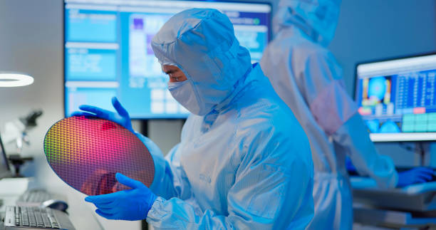
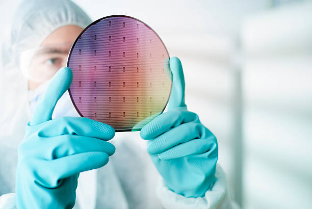
asian male technician in sterile coverall holds wafer that reflects many different colors with gloves and check it at semiconductor manufacturing plant
See also:
Close up shot of Silicon Wafer During Production at Advanced Semiconductor Foundry, that produces Microchips
Macro of many silicon Wafer with semiconductors in box inside clean room
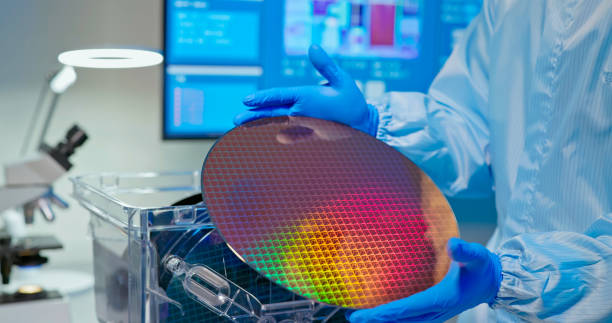
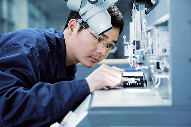
Lab worker examining a silicon wafer

Silicon chip wafer isolated on white.
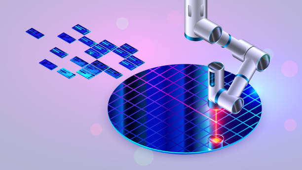
Semiconductor manufacturing with 3d rendering robotic arms with silicon wafers
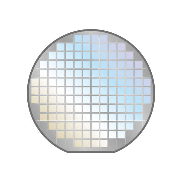

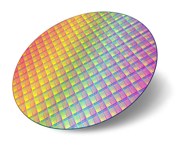
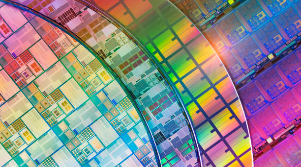
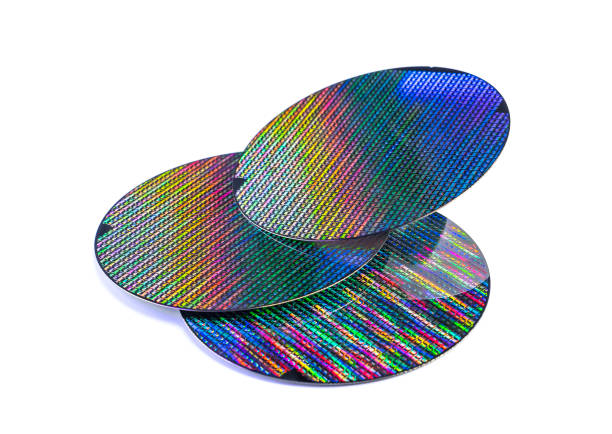
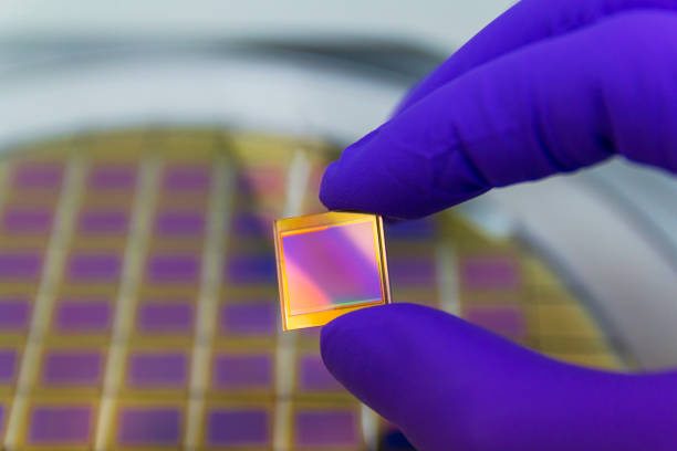
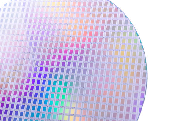
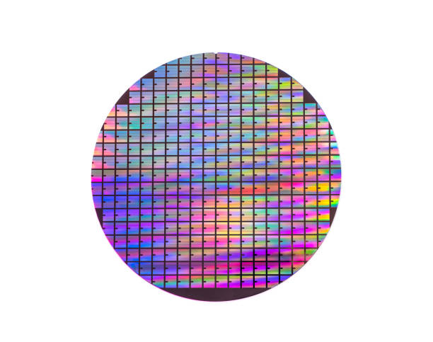
Isolated silicon wafer with hundreds of integrated circuits. Rainbow color patterns.

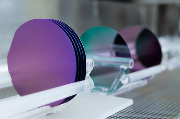
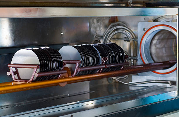
This is a set of 100 mm silicon wafers grown in a cleanroom facility. They are sitting in quartz holders or boats after being in a silicon dioxide growth furnace. The high heat from the furnace combined with oxygen converts the surface of the wafers to silicon dioxide. The wafer colors are dictated by the thickness of the silicon dioxide layer and the viewing angle. The purples and greens shown on these wafers are quite common and give the cleanroom a colorful and artistic touch.
Semiconductor manufacturing with 3d rendering robotic arms with silicon wafers

Semiconductor water isolated on white.
Computer, Service Occupation, CPU, Control, Education
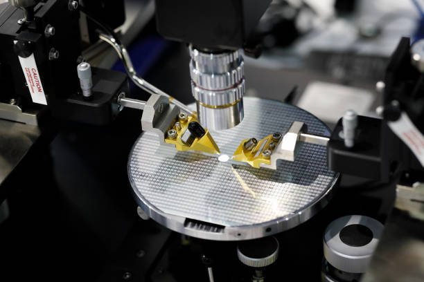
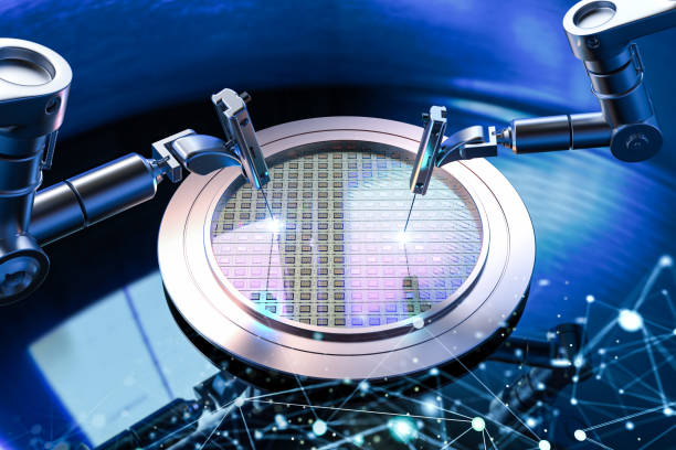
Manual probe system for RF test of semiconductor silicon wafers. Selective focus.
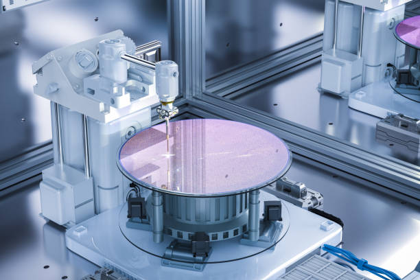
Semiconductor manufacturing with 3d rendering robotic arms with silicon wafers

3d rendering robotic arms with silicon wafers for semiconductor manufacturing
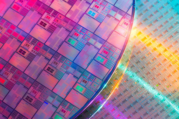
Hand in blue glove holding microchip photo sensor matrix . On the background is diced silicon wafer with microchips.Focus on chip.Close up.Rainbow on surface.
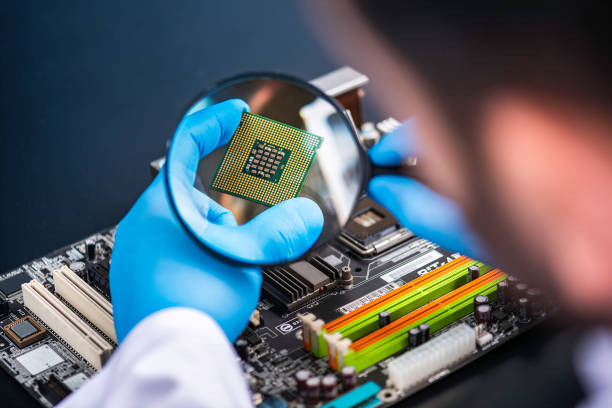
Nanotechnology, Computer Chip, CPU, Searching, Research
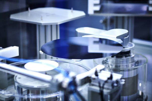
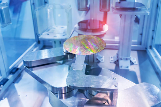
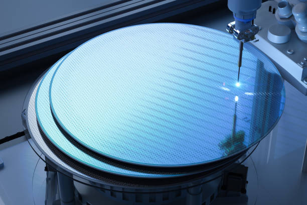
Close-up of computer wafer on robotic arm at production line in cleanroom.
CPU Silicon Wafer seen at 15x Magnification under UV lights.

IC wafer, electronic material, wafer, chip, bare core of electronic component
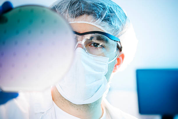
Lab worker examining a silicon wafer
Chip raw materials for mobile phones and integrated circuits
Silicon wafers on a horizontal batch reactor in a high-tech lab. Click on any of the sample images below to view all of my high-tech lab shots:

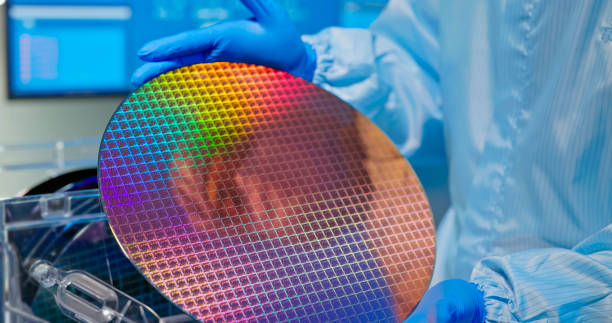
close up of asian male technician in sterile coverall holds wafer that reflects many different colors with gloves and check it at semiconductor manufacturing plant
close up of asian male technician in sterile coverall holds wafer that reflects many different colors with gloves and check it at semiconductor manufacturing plant
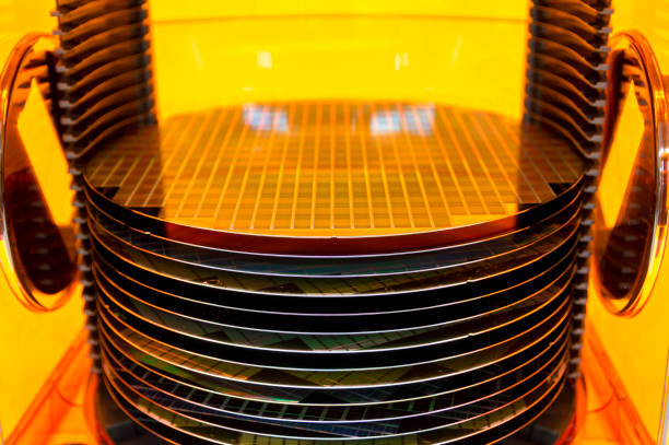
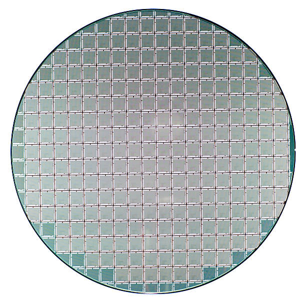
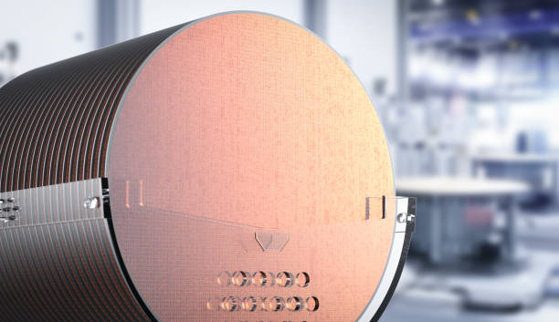
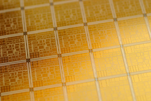
Shown are patterned 300 mm silicon wafers in a FOUP (front opening universal pod). Electronic circuit designs have been built onto the wafers using micromaching including photolithography. The FOUP is designed to interface with semiconductor processing equipment in a cleanroom fabrication facility.

Silicon wafer, starting point to make processors
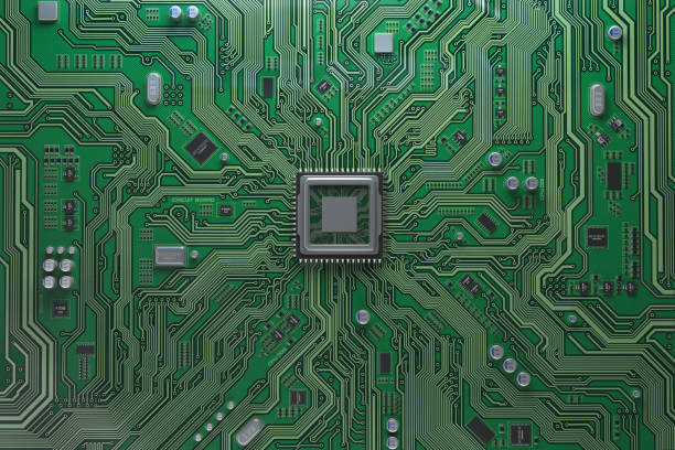
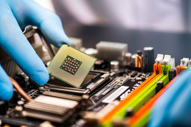
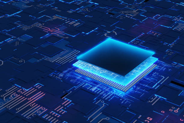
Computer motherboard with CPU. Circuit board system chip with core processor. Computer technology background. 3d illustration
3d rendering silicon wafer plates for semiconductor manufacturing
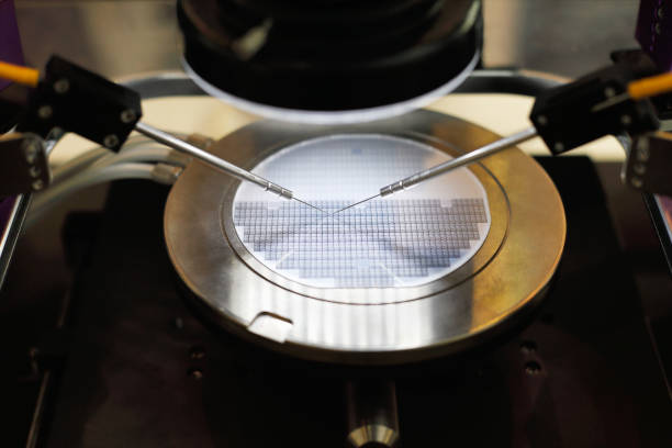
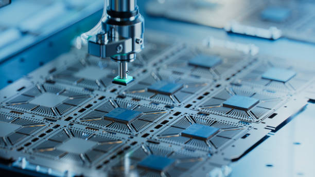
Semiconductor silicon wafer undergoing probe testing. Selective focus.
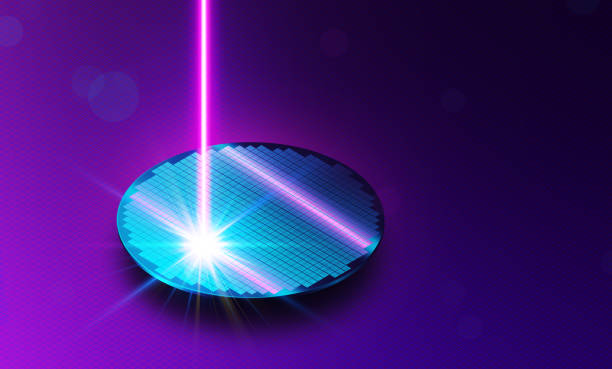
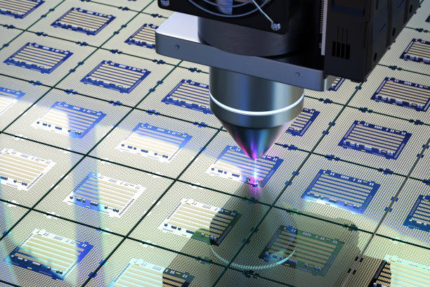
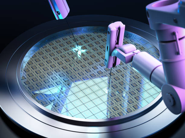
Extreme Ultraviolet Lithography Concept - EUV and EUVL - An EUV Laser Pulse Projecting Circuit Patterns onto a Silicon Wafer to Produce Next-Gen Microchips - 3D Illustration

Computer chip on mother board with visible working transistors layers, selective focus, CGI.
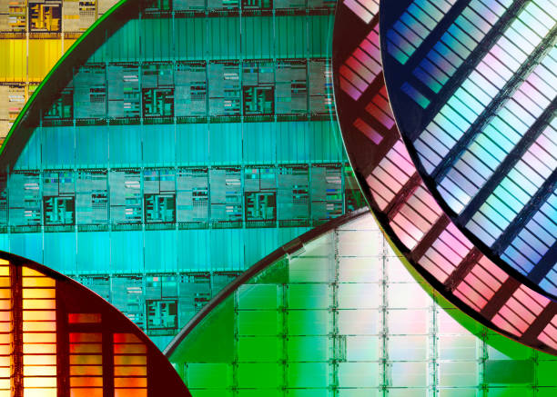
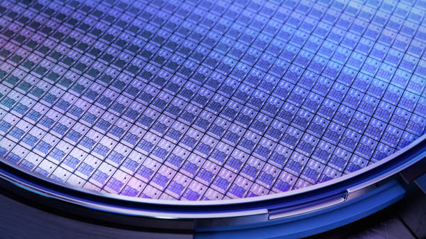
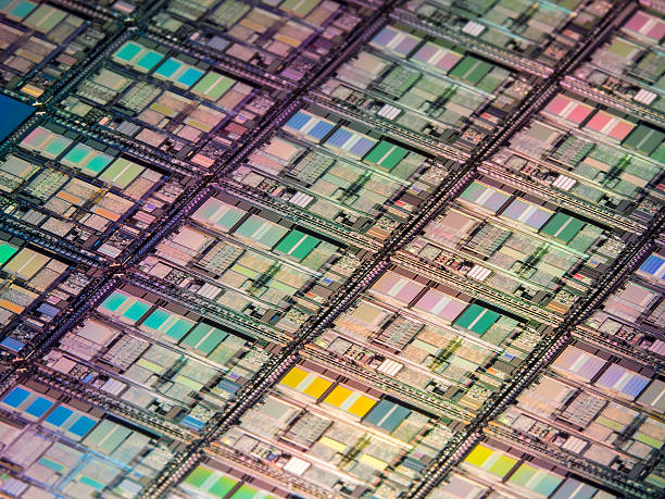
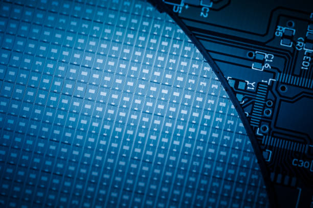
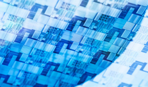
Silicon Wafers and Microcircuits - A wafer is a thin slice of semiconductor material, such as a crystalline silicon, used in electronics for the fabrication of integrated circuits.

asian male technician in sterile coverall holds wafer that reflects many different colors with gloves and check it at semiconductor manufacturing plant
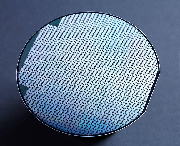
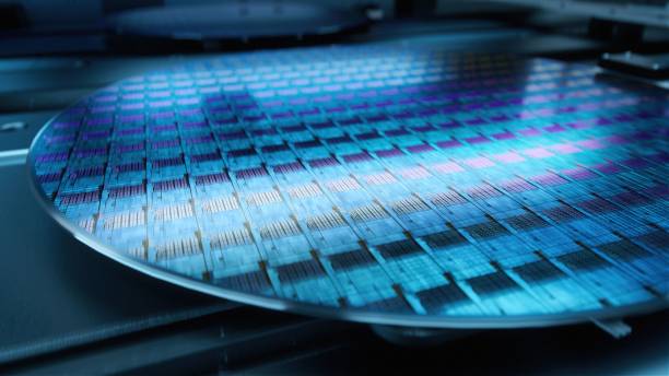
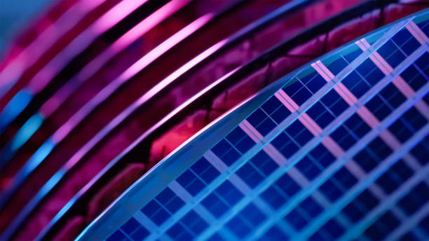
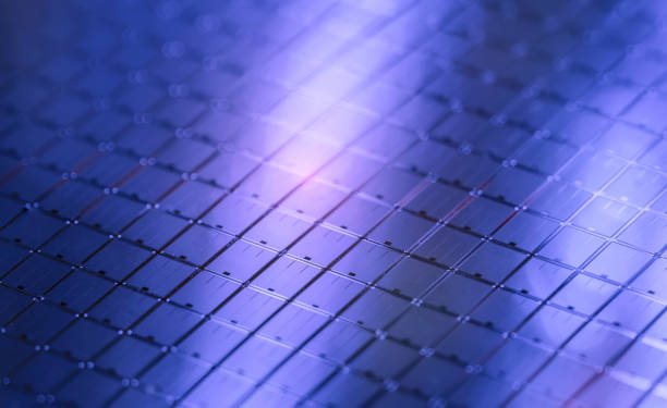
Macro of Silicon wafers

Worker or engineer wears medical protective suit or white coverall suit with silicon wafer
Next